Play with some interactive applications included on the SD Card.
Each of the applications below are also included in source format so you can see how they work in the Try page of this web site.
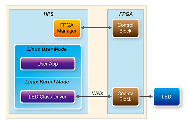
Blink The LEDs
There are two sets of LEDs connected to the SoC device. One LED is connected to a GPIO pin of the ARM processor, and eight others are connected to the FPGA I/O pins. This design controls the LEDs connected to the FPGA.
All On
All Off
Blink
Accelerometer (Persistence of Vision)
Description:
This application detects board movement by using the accelerometer connected via I2C interface to the CPU. As the board is shaken back and forth the LEDs are strobed to display, what our eyes detect as, an image.
Start
Stop
Use:
- Click the "Start" button to launch the application; the heartbeat LED will stop blinking.
- Important: Please disconnect the USB cable from the board to avoid damaging the connector during the next steps.
- Pick up the Atlas board so that the power cable is pointing towards you, and the LEDs are facing up.
- Wave the board left and right about 8 to 12 inches as fast as you can while focusing your eyes at the midpoint of the arc.
- You should see a pattern displayed by the 8 FPGA LEDs as they pass through the arc.
- When you are finished observing the PoV effect, reconnect the USB cable and click the “Stop” button (above).
- When you successfully stop the PoV demo, the heartbeat LED will begin flashing again.
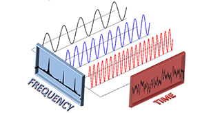
Fast Fourier Transform
This example design performs a 32-bit FFT on 3 waveform data sets, converting time domain data to frequency domain results. In this design, two processing methods are used:
- Hard Processor System (HPS): The 925 MHz dual-core ARM Cortex-A9 MPcore CPU and Neon co-processors are used to perform the FFT. The software uses optimized math libraries designed to exploit the power of the Neon co-processors.
- FPGA: A32-bit FFT hardware block inside the FPGA running at 100MHz is used to make the same mathematical transformation. DMA blocks in the FPGA read the raw data from the source location and write the results to the destination.
FFT Results
Using this application:
- Click a button to run the FFT on one of three data waveforms (sine, square, or triangle).
- The frequency domain plot will appear in the FFT Results panel on the right. The Performance Results (usec to calculate the FFT) are display in a table below.
- There are three data sets used: 256, 4k, and 1M samples. Each time you click a button it runs a different data set, then updates the plot and results tables. Note: The 1M sample plot is not displayed to minimize delay.
- FFTs are run using both the CPU and FPGA to illustrate the performance differences.
- Examples use data from two sources (RAM disk and FPGA) to model common system design choices. See the tabs below to learn more.
Sine Wave
Square Wave
Triangle Wave
Performance Results
Data Source in HPS
Data Source in FPGA
Number of samples in the FFT source data set:
CPU Processing (usec):
FPGA Processing (usec):
Time savings by processing in the FPGA (usec):
256
4,096
1,048,578
0
0
0
0
0
0
0
0
0
256
4,096
1,048,578
0
0
0
0
0
0
0
0
0
What the results show:
The numbers in the tables above show the time (in usec) it took to process the FFT sample data using the processor and FPGA. Twelve unique results are displayed covering all combinations of processing (CPU, FPGA), sample count (256, 4k, 1M), and source of the data (RAM disk, FPGA). The bottom row shows the difference between the CPU and FPGA processing in usec by subtracting the FPGA processing time from the CPU processing time. Positive values represent the amount time the CPU could use for other task when the FFT algorithm is handled by the FPGA.
How to interpret the data:
Processing: The CPU Processing row shows the performance of a 925MHz dual-core ARM Cortex-A9 MPCore processor with Neon co-processors, and optimized software libraries. The FPGA processing row shows the performance of using a 100MHz FFT hardware accelerator in the FPGA.
Data Source: There are two tables (red and blue) which show performance based on where the source data is located; in RAM disk or FPGA memory. The differences are due to the data transfer time between the data source and destination. The data source being in RAM disk is an advantage for the CPU; the data source being in the FPGA is an advantage for the FFT accelerator. Refer to the block diagrams below to see the data flow.
Number of Samples: For each waveform there are 3 data sets, each containing a different number of samples (256, 4k, 1M). With the smallest sample count (256) the CPU and FPGA performance results are nearly the same. This may seem odd since the FFT accelerator in the FPGA can process the data more quickly than the CPU, but there is some latency to fill the FFT accelerator pipeline. Once filled however, it is capable of generating a result on every clock. While the process of feeding the FFT accelerator and writing the results to RAM also adds latency, the performance results of the larger sample count waveforms clearly illustrate the advantage of using hardware accelleration.
Data Source in HPS
Data Source in FPGA
This example represents designs where the raw data is either generated by the CPU, or arrives via some processor interface (e.g. Ethernet).
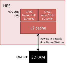
CPU Processing (925MHz dual-core CPU):
The processor reads the source data from the RAM disk, computes the FFT using software math libraries optimized for the Neon co-processors, then writes the results back to the RAM disk.
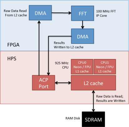
FPGA Processing (100MHz FFT core):
A DMA core inside the FPGA reads the data from RAM disk via the processor acceleration coherency port (ACP) and writes it to the FFT hardware block. A second DMA writes the results to the RAM disk via the ACP interface.
Since the ACP interface is used, both the raw and processed data are also directly available to the CPU via the L2 cache.
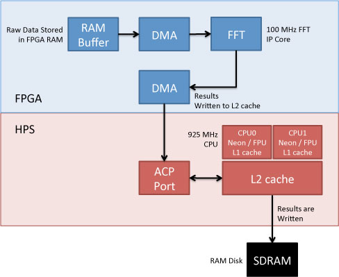
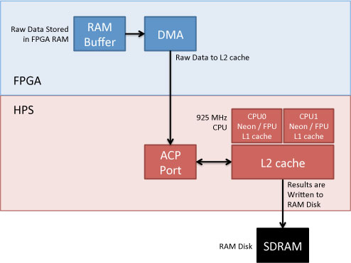
This example represents designs where the FPGA provides an interface to an external data source (e.g. A/D converter), or where logic within the FPGA generates the data.
CPU Processing (925MHz dual-core CPU):
A DMA core in the FPGA transfers the data directly to the CPU L2 cache via the acceleration coherency port (ACP). The CPU then runs the FFT and writes the results to RAM disk.
FPGA Processing (100MHz FFT Core):
One DMA core in the FPGA transfers the data directly to the the FFT hardware, while another writes the results to the RAM Disk via the acceleration coherency port (ACP).